
 NVIDIA Grace CPU is the first data center CPU developed by NVIDIA. It has been built from the ground up to create the world’s first superchips. Designed…
NVIDIA Grace CPU is the first data center CPU developed by NVIDIA. It has been built from the ground up to create the world’s first superchips.
Designed to deliver excellent performance and energy efficiency to meet the demands of modern data center workloads powering digital twins, cloud gaming and graphics, AI, and high-performance computing (HPC), NVIDIA Grace CPU features 72 Armv9 CPU cores that implement Arm Scalable Vector Extensions version two (SVE2) instruction set. The cores also incorporate virtualization extensions with nested virtualization capability and S-EL2 support.
NVIDIA Grace CPU is also compliant with the following Arm specifications:
- RAS v1.1 Generic Interrupt Controller (GIC) v4.1
- Memory Partitioning and Monitoring (MPAM)
- System Memory Management Unit (SMMU) v3.1
Grace CPU was built to pair with either the NVIDIA Hopper GPU to create the NVIDIA Grace CPU Superchip for large-scale AI training, inference, and HPC, or with another Grace CPU to build a high-performance CPU to meet the needs of HPC and cloud computing workloads.
Read on to learn about the key features of Grace CPU.
High-speed chip-to-chip interconnect with NVLink-C2C
Both the Grace Hopper and Grace Superchips are enabled by the NVIDIA NVLink-C2C high-speed chip-to-chip interconnect, which serves as the backbone for the superchip communication.
NVLink-C2C extends NVIDIA NVLink used to connect multiple GPUs in a server and, with NVLink Switch System, multiple GPU nodes.
With 900 GB/s of raw bidirectional bandwidth between dies on the package, NVLink-C2C provides 7x the bandwidth of a PCIe Gen 5 x16 link (the same bandwidth that is available between NVIDIA Hopper GPUs when using NVLink) and with lower latency. NVLink-C2C also requires just 1.3 picojoules/bit transferred, which is more than 5x the energy efficiency of PCIe Gen 5.
NVLink-C2C is also a coherent interconnect, which enables coherency when programming both a standard coherent CPU platform using the Grace CPU Superchip, as well as a heterogeneous programming model with the Grace Hopper Superchip.
Standards-compliant platforms with NVIDIA Grace CPU
NVIDIA Grace CPU Superchip is built to provide software developers with a standards-compliant platform. Arm provides a set of specifications as part of its System Ready initiative, which aims to bring standardization to the Arm ecosystem.
Grace CPU targets the Arm system standards to offer compatibility with off-the-shelf operating systems and software applications, and Grace CPU will take advantage of the NVIDIA Arm software stack from the start.
Grace CPU also complies with the Arm Server Base System Architecture (SBSA) to enable standards-compliant hardware and software interfaces. In addition, to enable standard boot flows on Grace CPU-based systems, Grace CPU has been designed to support Arm Server Base Boot Requirements (SBBR).
For cache and bandwidth partitioning, as well as bandwidth monitoring, Grace CPU also supports Arm Memory Partitioning and Monitoring (MPAM).
Grace CPU also includes Arm Performance Monitoring Units, allowing for the performance monitoring of the CPU cores as well as other subsystems in the system-on-a-chip (SoC) architecture. This enables standard tools, such as Linux perf, to be used for performance investigations.
Unified Memory with Grace Hopper Superchip
Combining a Grace CPU with a Hopper GPU, the NVIDIA Grace Hopper Superchip expands upon the CUDA Unified Memory programming model that was first introduced in CUDA 8.0.
NVIDIA Grace Hopper Superchip introduces Unified Memory with shared page tables, allowing the Grace CPU and Hopper GPU to share an address space and even page tables with a CUDA application.
The Grace Hopper GPU can also access pageable memory allocations. Grace Hopper Superchip allows programmers to use system allocators to allocate GPU memory, including the ability to exchange pointers to malloc memory with the GPU.
NVLink-C2C enables native atomic support between the Grace CPU and the Hopper GPU, unlocking the full potential for C++ atomics that were first introduced in CUDA 10.2.
NVIDIA Scalable Coherency Fabric
Grace CPU introduces the NVIDIA Scalable Coherency Fabric (SCF). Designed by NVIDIA, SCF is a mesh fabric and distributed cache designed to scale to the needs of the data center. SCF provides 3.2 TB/s of bisection bandwidth to ensure the flow of data traffic between NVLink-C2C, CPU cores, memory, and system IOs.
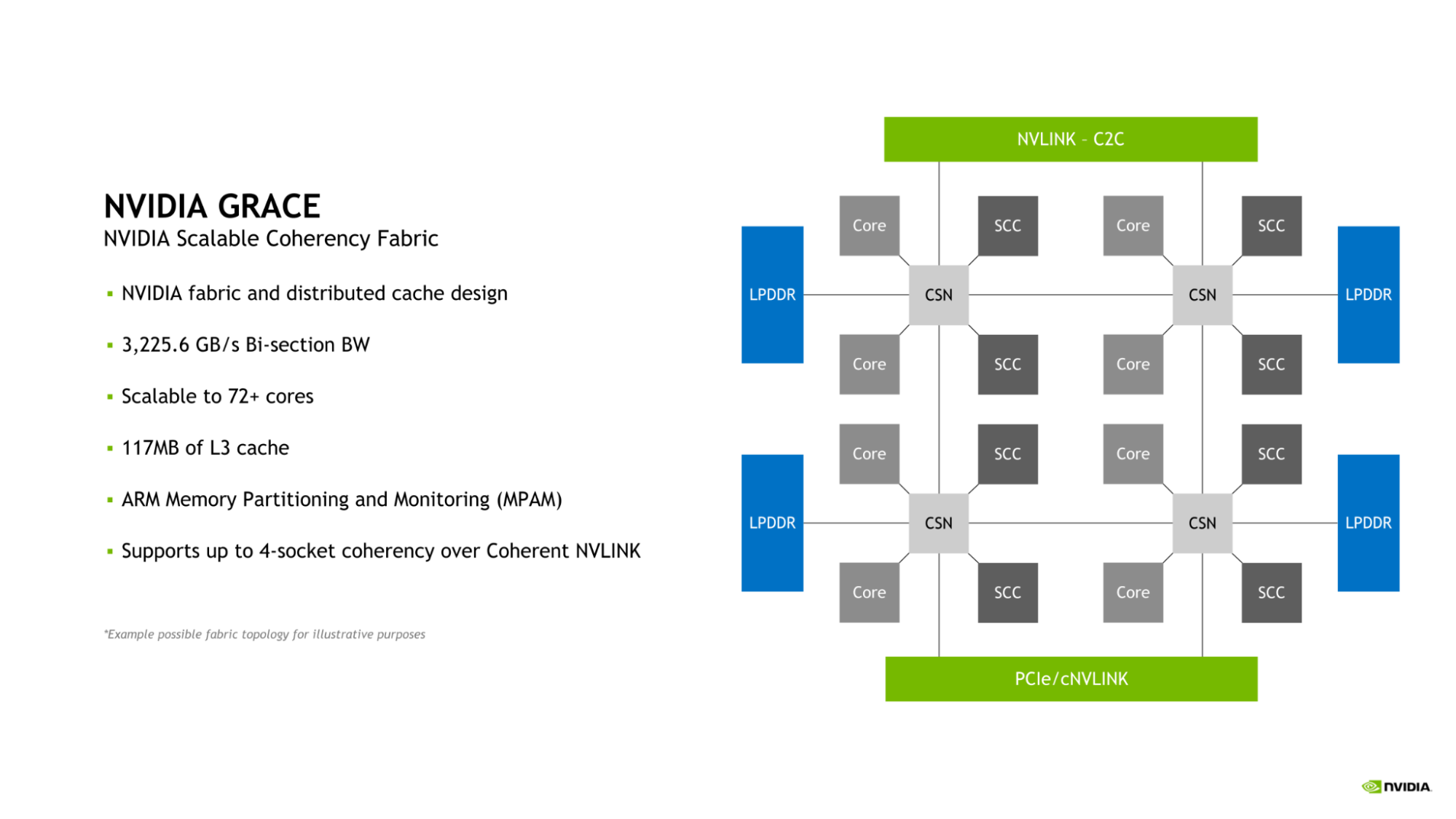
A single Grace CPU incorporates 72 CPU cores and 117 MB of cache, but SCF is designed for scalability beyond this configuration. When two Grace CPUs are combined to form a Grace Superchip, these figures double to 144 CPU cores and 234 MB of L3 cache, respectively.
The CPU cores and SCF Cache partitions (SCCs) are distributed throughout the mesh. Cache Switch Nodes (CSNs) route data through the fabric and serve as interfaces between the CPU cores, cache memory and the rest of the system, enabling high-bandwidth throughout.
Memory partitioning and monitoring
Grace CPU incorporates support for Memory System Resource Partitioning and Monitoring (MPAM) capability, which is the Arm standard for partitioning both system cache and memory resources.
MPAM works by assigning partition IDs (PARTIDs) to requestors within the system. This design allows resources such as cache capacity and memory bandwidth to be partitioned or monitored based on their respective PARTIDs.
The SCF Cache in Grace CPU supports both the partitioning of cache capacity as well as memory bandwidth using MPAM. Additionally, Performance Monitor Groups (PMGs) can be used to monitor resource usage.
Boosting bandwidth and energy efficiency with memory subsystem
To deliver excellent bandwidth and energy efficiency, Grace CPU implements a 32-channel LPDDR5X memory interface. This provides memory capacity of up to 512 GB and memory bandwidth of up to 546 GB/s.
Extended GPU Memory
A key feature of the Grace Hopper Superchip is the introduction of Extended GPU Memory (EGM). By allowing any Hopper GPU connected from a larger NVLink network to access the LPDDR5X memory connected to the Grace CPU in the Grace Hopper Superchip, the memory pool available to the GPU is greatly expanded.
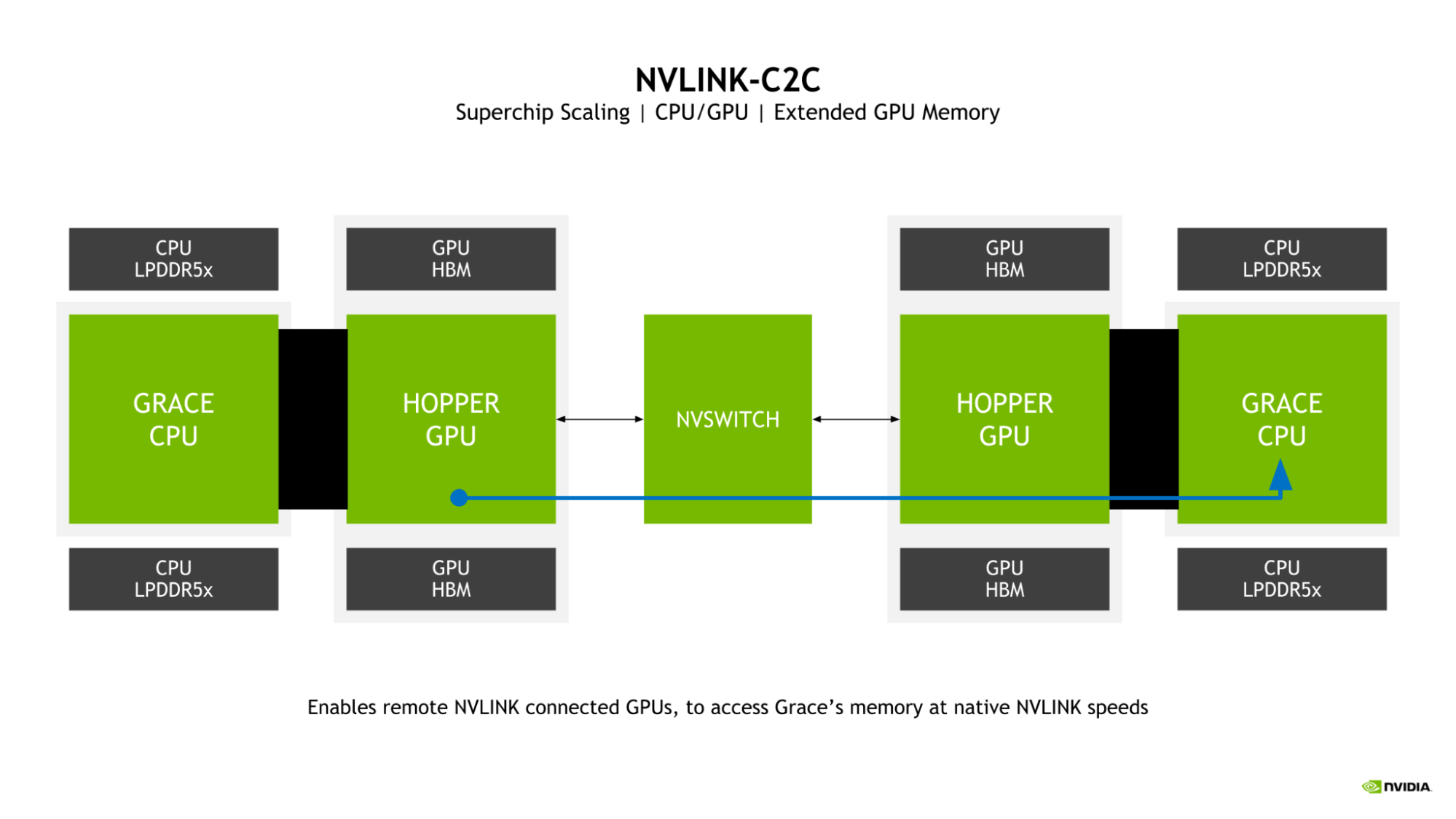
The GPU-to-GPU NVLink and NVLink-C2C bidirectional bandwidths are matched in a superchip, which enables the Hopper GPUs to access the Grace CPU memory at NVLink native speeds.
Balancing bandwidth and energy efficiency with LPDDR5X
The selection of LPDDR5X for Grace CPU was driven by the need to strike the optimal balance of bandwidth, energy efficiency, capacity, and cost for large-scale AI and HPC workloads.
While a four-site HBM2e memory subsystem would have provided substantial memory bandwidth and good energy efficiency, it would do so at more than 3x the cost-per-gigabyte of either DDR5 or LPDDR5X.
Additionally, such a configuration would be limited to a capacity of only 64 GB, which is one-eighth the maximum capacity available to the Grace CPU with LPDDR5X.
Compared to a more traditional eight-channel DDR5 design, the Grace CPU LPDDR5X memory subsystem provides up to 53% more bandwidth and is substantially more power efficient, requiring just an eighth of the power per gigabyte.
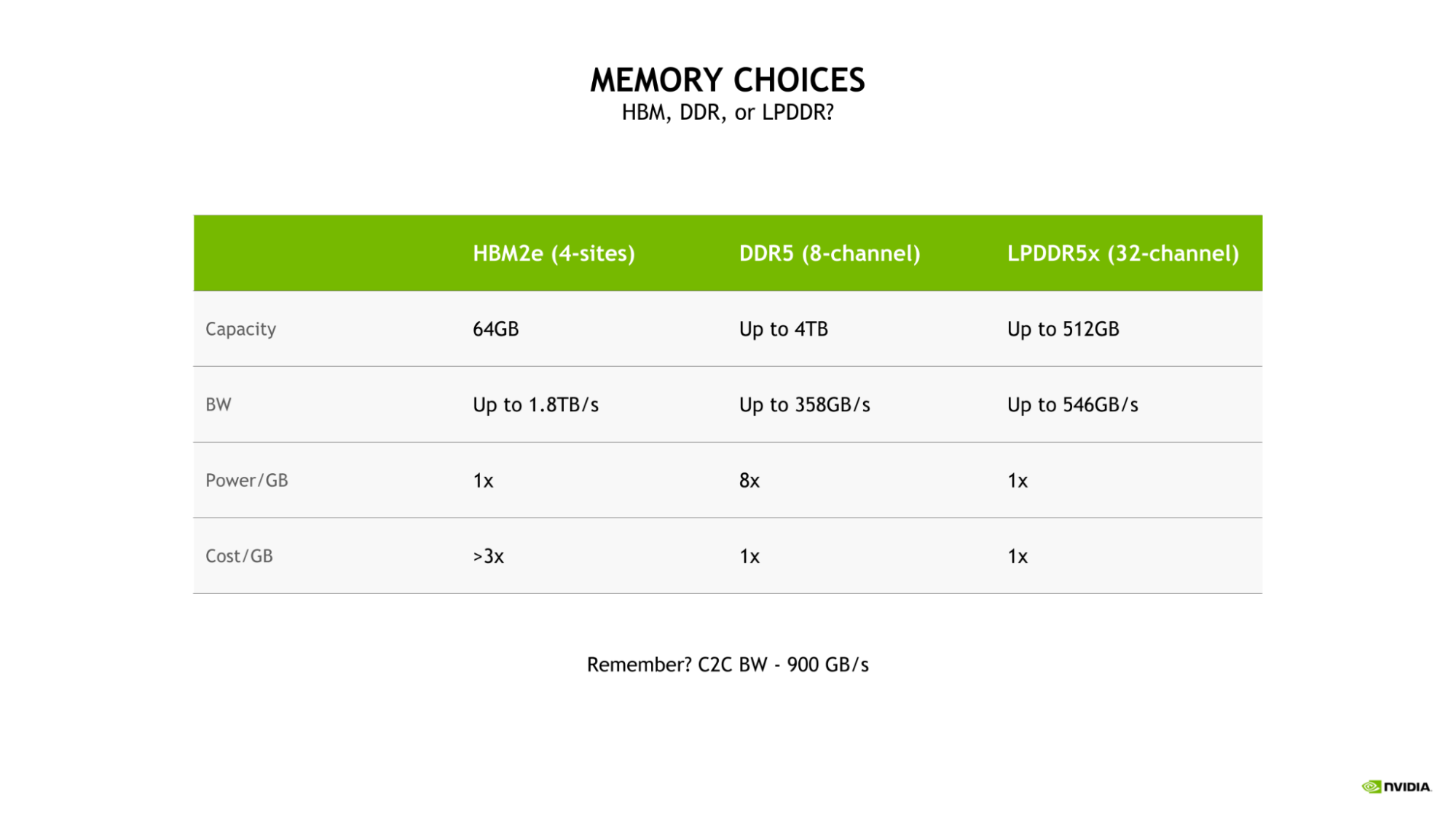
The excellent power efficiency of LPDDR5X enables allocating more of the total power budget to compute resources, such as the CPU cores or GPU streaming multiprocessors (SMs).
NVIDIA Grace CPU I/O
Grace CPU incorporates a complement of high-speed I/O to serve the needs of the modern data center. The Grace CPU SoC provides up to 68 lanes of PCIe connectivity and up to four PCIe Gen 5 x16 links. Each PCIe Gen 5 x16 link offers up to 128 GB/s of bidirectional bandwidth and can be further bifurcated into two PCIe Gen 5 x8 links for additional connectivity.
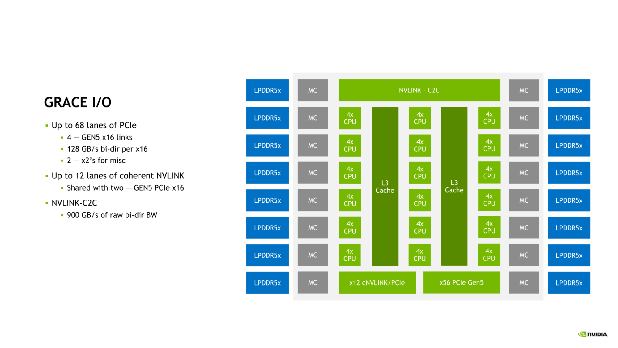
This connectivity is in addition to the on-die NVLink-C2C link that can be used to connect Grace CPU to either another Grace CPU or to an NVIDIA Hopper GPU.
The combination of NVLink, NVLink-C2C, and PCIe Gen 5 provides the Grace CPU with the rich suite of connectivity options and ample bandwidth needed to scale performance in the modern data center.
NVIDIA Grace CPU performance
NVIDIA Grace CPU is designed to deliver excellent compute performance in both single-chip as well as Grace Superchip configurations, with estimated SPECrate2017_int_base scores of 370 and 740, respectively. These pre-silicon estimates are based on use of the GNU Compiler Collection (GCC).

Memory bandwidth is critical to the workloads for which the Grace CPU was designed, and in the Stream Benchmark, a single Grace CPU is expected to deliver up to 536 GB/s of realized bandwidth, representing more than 98% of the chip’s peak theoretical bandwidth.

And, finally, the bandwidth between the Hopper GPU and the Grace CPU is critical to maximizing the performance of the Grace Hopper Superchip. GPU-to-CPU memory reads and writes are expected to be 429 GB/s and 407 GB/s, respectively, representing more than 95% and more than 90% of the peak theoretical unidirectional transfer rates of NVLink-C2C.
Combined read and write performance is expected to be 506 GB/s, representing over 92% of the peak theoretical memory bandwidth available to a single NVIDIA Grace CPU SoC.

Benefits of the NVIDIA Grace CPU Superchip
With 144 cores and 1 TB/s of memory bandwidth, the NVIDIA Grace CPU Superchip will provide unprecedented performance for CPU-based high performance computing applications. HPC applications are compute-intensive, demanding the highest-performing cores, highest-memory bandwidth, and the right memory capacity per core to speed outcomes.
NVIDIA is working with leading HPC, supercomputing, hyperscale, and cloud customers for the Grace CPU Superchip. Grace CPU Superchip and Grace Hopper Superchip are expected to be available in the first half of 2023.
For more information about the NVIDIA Grace Hopper Superchip and NVIDIA Grace CPU Superchip, visit NVIDIA Grace CPU.