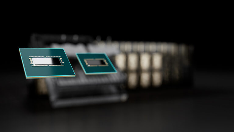
 Increasing demands in AI and high-performance computing (HPC) are driving a need for faster, more scalable interconnects with high-speed communication between…
Increasing demands in AI and high-performance computing (HPC) are driving a need for faster, more scalable interconnects with high-speed communication between every GPU.
The third-generation NVIDIA NVSwitch is designed to satisfy this communication need. This latest NVSwitch and the H100 Tensor Core GPU use the fourth-generation NVLink, the newest high-speed, point-to-point interconnect by NVIDIA.
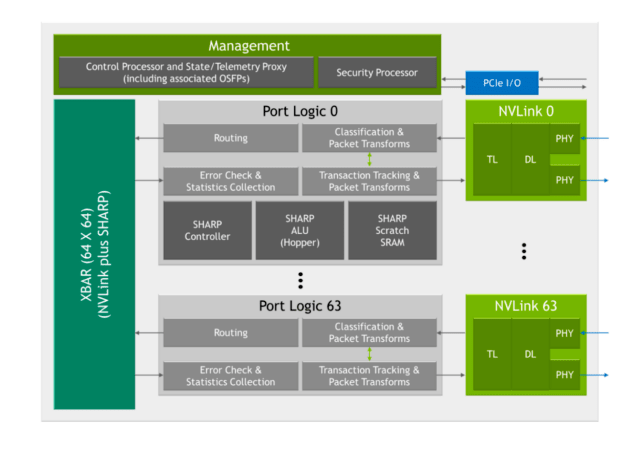
The third-generation NVIDIA NVSwitch is designed to provide connectivity within a node or to GPUs external to the node for the NVLink Switch System. It also incorporates hardware acceleration for collective operations with multicast and NVIDIA Scalable Hierarchical Aggregation and Reduction Protocol (SHARP) in-network reductions.
NVIDIA NVSwitch is also a critical enabler of the NVLink Switch networking appliance, which enables the creation of clusters with up to 256 connected NVIDIA H100 Tensor Core GPUs and 57.6 TB/s of all-to-all bandwidth. The appliance delivers 9x more bisection bandwidth than was possible with HDR InfiniBand on NVIDIA Ampere Architecture GPUs.
High bandwidth and GPU-compatible operation
The performance needs of AI and HPC workloads continue to grow rapidly and require scaling to multi-node, multi-GPU systems.
Delivering excellent performance at scale requires high-bandwidth communication between every GPU, and the NVIDIA NVLink specification is designed for synergistic operation with NVIDIA GPUs to enable the required performance and scalability.
For instance, the thread-block execution structure of NVIDIA GPUs efficiently feeds the parallelized NVLink architecture. NVLink-Port interfaces have also been designed to match the data exchange semantics of GPU L2 caches as closely as possible.
Faster than PCIe
A key benefit of NVLink is that it offers substantially greater bandwidth than PCIe. Fourth-generation NVLink is capable of 100 Gbps per lane, more than tripling the 32 Gbps bandwidth of PCIe Gen5. Multiple NVLinks can be combined to provide even higher aggregate lane counts, yielding higher throughput.
Lower overhead than traditional networks
NVLink has been designed specifically as a high-speed, point-to-point link to interconnect GPUs, yielding lower overhead than would be present in traditional networks.
This enables many of the complex networking features found in traditional networks—such as end-to-end retry, adaptive routing, and packet reordering—to be traded off for increased port counts.
The greater simplicity of the network interface allows for application–, presentation–, and session-layer functionality to be embedded directly into CUDA itself, further reducing communication overhead.
NVLink generations
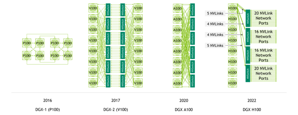
First introduced with the NVIDIA P100 GPU, NVLink has continued to advance in lockstep with NVIDIA GPU architectures, with each new architecture accompanied by a new generation of NVLink.
Fourth-generation NVLink provides 900 GB/s of bidirectional bandwidth per GPU—1.5x greater than the prior generation and more than 5.6x higher than first-generation NVLink.
NVLink-enabled server generations
NVIDIA NVSwitch was first introduced with the NVIDIA V100 Tensor Core GPU and second-generation NVLink, enabling high-bandwidth, any-to-any connectivity between all GPUs in a server.
The NVIDIA A100 Tensor Core GPU introduced third-generation NVLink and second-generation NVSwitch, doubling both per-GPU bandwidth as well as reduction bandwidth.
With fourth-generation NVLink and third-generation NVSwitch, a system with eight NVIDIA H100 Tensor Core GPUs features 3.6 TB/s of bisection bandwidth and 450 GB/s of bandwidth for reduction operations. These are1.5x and 3x increases compared to the prior generation.
In addition, with fourth-generation NVLink and third-generation NVSwitch as well as the external NVIDIA NVLink Switch, multi-GPU communication across multiple servers at NVLink speeds is now possible.
The largest and fastest switch chip to date
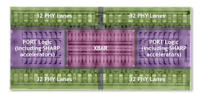
Third-generation NVSwitch is the largest NVSwitch to date. It is built using the TSMC 4N process customized for NVIDIA. The die incorporates 25.1 billion transistors—more transistors than the NVIDIA V100 Tensor Core GPU—in an area of 294 mm2. The package dimensions are 50 mm x 50 mm with a total of 2645 solder balls.
NVLink network support
Third-generation NVSwitch is a key enabler of the NVLink Switch System, which enables connectivity between GPUs across nodes at NVLink speeds.
It incorporates physical (PHY) electrical interfaces that are compatible with 400 Gbps Ethernet and InfiniBand connectivity. The included management controller now provides support for attached Octal Small Formfactor Pluggable (OSFP) modules with four NVLinks per cage. With custom firmware, active cables can be supported.
Additional forward error correction (FEC) modes have also been added to enhance NVLink Network performance and reliability.
A security processor has also been added to protect data and chip configuration from attacks. The chip provides partitioning features that can isolate subsets of ports into separate NVLink Networks. Expanded telemetry features also enable InfiniBand-style monitoring.
Double the bandwidth
Third-generation NVSwitch is our highest-bandwidth NVSwitch yet.
With 100 Gbps of bandwidth per differential pair using 50 Gbaud PAM4 signaling, third-generation NVSwitch provides 3.2 TB/s of full-duplex bandwidth across 64 NVLink ports (x2 per NVLink). It delivers more bandwidth in a system while also requiring fewer NVSwitch chips compared to the prior generation. All ports on third-generation NVSwitch are NVLink Network–capable.
SHARP collectives and multicast support
Third-generation NVSwitch includes a host of new hardware blocks for SHARP acceleration:
- A SHARP controller
- SHARP arithmetic logic units (ALUs) highly leveraged from those in the NVIDIA Hopper Architecture
- Embedded SRAM to support the SHARP calculations
The embedded ALUs offer up to 400 FLOPS of FP32 throughput and have been added to perform reduction operations directly in NVSwitch, rather than by the GPUs in the system.
These ALUs support a wide variety of operators, such as logical, min/max, and add. They also support data formats such as signed/unsigned integers, FP16, FP32, FP64, and BF16.
Third-generation NVSwitch also includes a SHARP controller that can manage up to 128 SHARP groups in parallel. The crossbar bandwidth in the chip has been increased to carry additional SHARP-related exchanges.
all-reduce operation compatibility
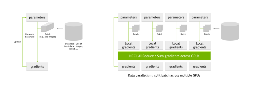
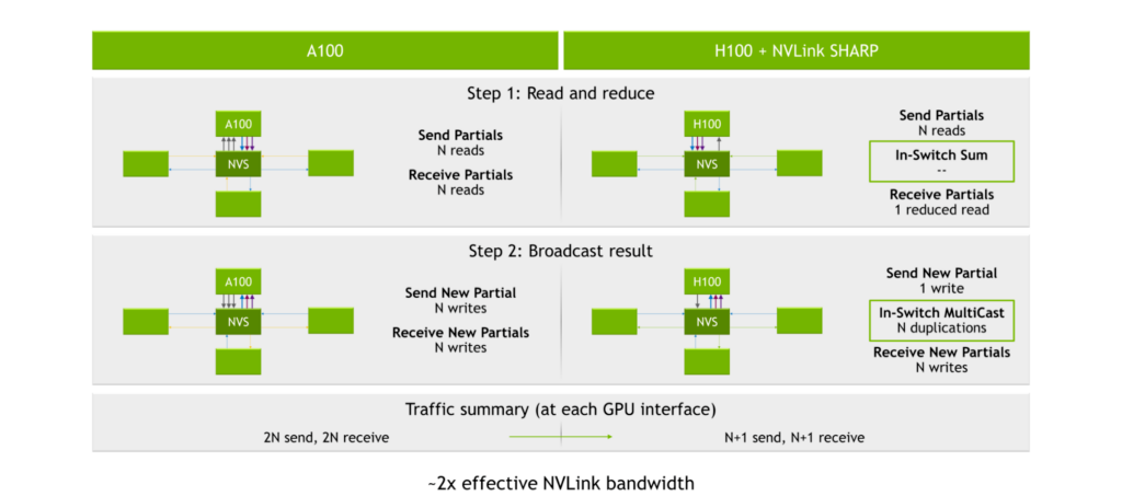
A key use case for NVIDIA SHARP is for all-reduce operations that are common in AI training. When training networks using multiple GPUs, batches are split into smaller subbatches, which are then assigned to each individual GPU.
Each GPU processes their individual subbatches through the network parameters, yielding possible changes to the parameters, also known as local gradients. These local gradients are combined and reconciled to produce global gradients, which each GPU applies to their parameter tables. This averaging process is also known as an all-reduce operation.
NVIDIA Magnum IO is the architecture for data center IO to accelerate multi-GPU and multi-node communications. It enables HPC, AI, and scientific applications to scale performance on new large GPU clusters scaled using NVLink and NVSwitch.
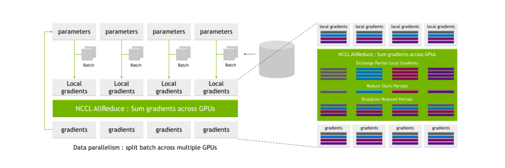
Magnum IO includes the NVIDIA Collective Communication Library (NCCL), which implements a wealth of multi-GPU and multi-node collective primitives, including all-reduce.
NCCL AllReduce takes as input the local gradients, partitions them into subsets, collects all subsets of a certain level and assigns it to a single GPU. The GPU then performs the reconciliation process for that subset, such as summing across local gradient values from all GPUs.
Following this process, a global set of gradients is produced and then distributed to all other GPUs.
These processes are highly communication-intensive and the associated communication overhead can substantially lengthen the overall time to train.
With the NVIDIA A100 Tensor Core GPU, third-generation NVLink, and second-generation NVSwitch, the process of sending and receiving partials yields 2N reads (where N is the number of GPUs). The process of broadcasting results yields 2N writes for 2N reads and 2N writes at each GPU interface, or 4N total operations.
The SHARP engines are inside of third-generation NVSwitch. Instead of distributing the data to each GPU and having the GPUs perform the calculations, the GPUs send their data into third-generation NVSwitch chips. The chips then perform the calculations and then send the results back. This results in a total of 2N+2 operations, or approximately halving the number of read/write operations needed to perform the all-reduce calculation.
Boosting performance for large-scale models
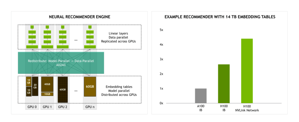
With the NVLink Switch System providing 4.5x more bandwidth than InfiniBand, large-scale model training becomes more practical.
For example, when training a recommendation engine with 14 TB embedding tables, we expect a significant performance uplift in performance for H100 using the NVLink Switch System compared to H100 using InfiniBand.
NVLink Network
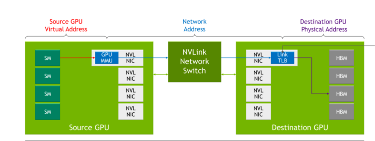
In prior generations of NVLink, each server had its own local address space used by GPUs within a server when communicating to each other over NVLink. With the NVLink Network, each server has its own address space, which is used when GPUs send data across the network, providing isolation and improved security when sharing data. This capability leverages functionality built into the latest NVIDIA Hopper GPU Architecture.
While NVLink performs connection setup during the system boot process, the NVLink Network connection setup is performed through a runtime API call by software. This enables the network to be reconfigured on the fly as different servers come online and as users enter and exit.
Table 1 shows how traditional networking concepts map to their counterparts in NVLink Network.
| Concept | Traditional Example | NVLink Network |
| Physical Layer | 400G electrical/optical media | Custom-FW OSFP |
| Data Link Layer | Ethernet | NVLink custom on-chip HW and FW |
| Network Layer | IP | New NVLink Network Addressing and Management Protocols |
| Transport Layer | TCP | NVLink custom on-chip HW and FW |
| Session Layer | Sockets | SHARP groupsCUDA export of Network addresses of data-structures |
| Presentation Layer | TSL/SSL | Library abstractions (e.g., NCCL, NVSHMEM) |
| Application Layer | HTTP/FTP | AI Frameworks or User Apps |
| NIC | PCIe NIC (card or chip) | Functions embedded in GPU and NVSwitch |
| RDMA Off-Load | NIC Off-Load Engine | GPU-internal Copy Engine |
| Collectives Off-Load | NIC/Switch Off-Load Engine | NVSwitch-internal SHARP Engines |
| Security Off-Load | NIC Security Features | GPU-internal Encryption and “TLB” Firewalls |
| Media Control | NIC Cable Adaptation | NVSwitch-internal OSFP-cable controllers |
DGX H100
NVIDIA DGX H100 is the latest iteration of the DGX family of systems based on the latest NVIDIA H100 Tensor Core GPU and incorporates:
- 8x NVIDIA H100 Tensor Core GPUs with 640GB of aggregate GPU memory
- 4x third-generation NVIDIA NVSwitch chips
- 18x NVLink Network OSFPs
- 3.6 TB/s of full-duplex NVLink Network bandwidth provided by 72 NVLinks
- 8x NVIDIA ConnectX-7 Ethernet/InfiniBand ports
- 2x dual-port BlueField-3 DPUs
- Dual Sapphire Rapids CPUs
- Support for PCIe Gen 5
Full bandwidth intra-server NVLink
Within a DGX H100, each of the eight H100 Tensor Core GPUs within the system is connected to all four third-generation NVSwitch chips. Traffic is sent across four different switch planes, enabling the aggregation of the links to achieve full all-to-all bandwidth between GPUs in the system.
Half-bandwidth NVLink Network
With NVLink Network, all eight NVIDIA H100 Tensor Core GPUs within a server can half-subscribe 18 NVLinks to H100 Tensor Core GPUs in other servers.
Alternatively, four H100 Tensor Core GPUs in a server can fully subscribe 18 NVLinks to H100 Tensor Core GPUs in other servers. This 2:1 taper is a trade-off made to balance bandwidth with server complexity and cost for this instantiation of the technology.
With SHARP, the bandwidth delivered is equivalent to a full-bandwidth AllReduce.
Multi-rail Ethernet
Within a server, all eight GPUs independently support RDMA from their own dedicated 400 GB NICs. 800 GB/s of aggregate full-duplex bandwidth is possible to non-NVLink Network devices.
DGX H100 SuperPOD
DGX H100 is the building block of the DGX H100 SuperPOD.
- Built from eight compute racks, each with four DGX H100 servers.
- Features a total of 32 DGX H100 nodes, incorporating 256 NVIDIA H100 Tensor Core GPUs.
- Delivers up to a peak of one exaflop of peak AI compute.
The NVLink Network provides 57.6 TB/s bisection bandwidth spanning the entire 256 GPUs. Additionally, the ConnectX-7s across all 32 DGXs and associated InfiniBand switches provide 25.6 TB/s of full duplex bandwidth for use within the pod or for scaling out the multiple SuperPODs.
NVLink Switch
A key enabler of DGX H100 SuperPOD is the new NVLink Switch based on the third-generation NVSwitch chips. DGX H100 SuperPOD includes 18 NVLink Switches.
The NVLink Switch fits in a standard 1U 19-inch form factor, significantly leveraging InfiniBand switch design, and includes 32 OSFP cages. Each switch incorporates two third-generation NVSwitch chips, providing 128 fourth-generation NVLink ports for an aggregate 6.4 TB/s full-duplex bandwidth.
NVLink Switch supports out-of-band management communication and a range of cabling options such as passive copper. With custom firmware, active copper and optical OSFP cables are also supported.
Scale up with NVLink Network
H100 SuperPOD with NVLink Network enables significant increases in bisection and reduce operation bandwidth compared to a DGX A100 SuperPOD with 256 DGX A100
GPUs.
A single DGX H100 delivers 1.5x the bisection and 3x the bandwidth for reduction operations of a single DGX A100. Those speedups grow to 9x and 4.5x in 32 DGX system configurations, each with a total of 256 GPUs.
Performance benefits for communication-intensive workloads
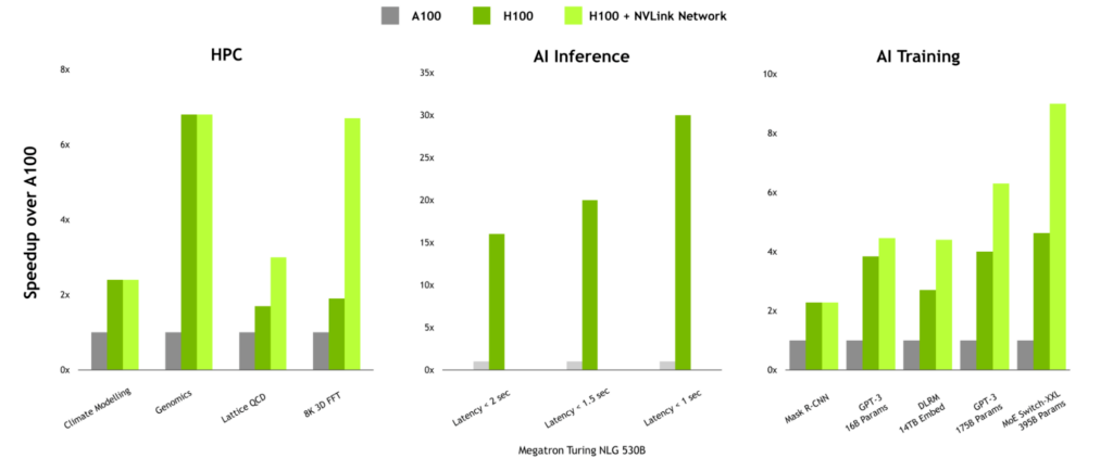
For workloads with high communication intensity, the performance benefits of NVLink Network can be significant. In HPC, workloads such as Lattice QCD and 8K 3D FFT see substantial benefits because multi-node scaling has been designed into the communication libraries within the HPC SDK and Magnum IO.
NVLink Network can also provide a significant boost when training large language models or recommenders with large embedding tables.
Delivering performance at scale
Delivering the highest performance for AI and HPC requires full-stack, data-center scale innovation. High-bandwidth, low-latency interconnect technologies are key enablers of performance at scale.
Third-generation NVSwitch delivers the next big leap for high-bandwidth, low-latency communication between GPUs both within a server, as well as bringing all-to-all GPU communication at full NVLink speed between server nodes.
Magnum IO works integrally with CUDA, HPC SDK, and nearly all deep learning frameworks. It enables AI software—such as large language models, recommender systems, and scientific applications like 3D FFT—to scale across multiple GPUs across multiple nodes using NVLink Switch System right out of the box.
For more information, see NVIDIA NVLink and NVSwitch.


