 Learn about the latest RTX and neural rendering technologies and how they are accelerating game development.
Learn about the latest RTX and neural rendering technologies and how they are accelerating game development.
 DataBloom
Learn about the latest RTX and neural rendering technologies and how they are accelerating game development.
Learn about the latest RTX and neural rendering technologies and how they are accelerating game development.
 NVIDIA Grace CPU is the first data center CPU developed by NVIDIA. It has been built from the ground up to create the world’s first superchips. Designed…
NVIDIA Grace CPU is the first data center CPU developed by NVIDIA. It has been built from the ground up to create the world’s first superchips.
Designed to deliver excellent performance and energy efficiency to meet the demands of modern data center workloads powering digital twins, cloud gaming and graphics, AI, and high-performance computing (HPC), NVIDIA Grace CPU features 72 Armv9 CPU cores that implement Arm Scalable Vector Extensions version two (SVE2) instruction set. The cores also incorporate virtualization extensions with nested virtualization capability and S-EL2 support.
NVIDIA Grace CPU is also compliant with the following Arm specifications:
Grace CPU was built to pair with either the NVIDIA Hopper GPU to create the NVIDIA Grace CPU Superchip for large-scale AI training, inference, and HPC, or with another Grace CPU to build a high-performance CPU to meet the needs of HPC and cloud computing workloads.
Read on to learn about the key features of Grace CPU.
Both the Grace Hopper and Grace Superchips are enabled by the NVIDIA NVLink-C2C high-speed chip-to-chip interconnect, which serves as the backbone for the superchip communication.
NVLink-C2C extends NVIDIA NVLink used to connect multiple GPUs in a server and, with NVLink Switch System, multiple GPU nodes.
With 900 GB/s of raw bidirectional bandwidth between dies on the package, NVLink-C2C provides 7x the bandwidth of a PCIe Gen 5 x16 link (the same bandwidth that is available between NVIDIA Hopper GPUs when using NVLink) and with lower latency. NVLink-C2C also requires just 1.3 picojoules/bit transferred, which is more than 5x the energy efficiency of PCIe Gen 5.
NVLink-C2C is also a coherent interconnect, which enables coherency when programming both a standard coherent CPU platform using the Grace CPU Superchip, as well as a heterogeneous programming model with the Grace Hopper Superchip.
NVIDIA Grace CPU Superchip is built to provide software developers with a standards-compliant platform. Arm provides a set of specifications as part of its System Ready initiative, which aims to bring standardization to the Arm ecosystem.
Grace CPU targets the Arm system standards to offer compatibility with off-the-shelf operating systems and software applications, and Grace CPU will take advantage of the NVIDIA Arm software stack from the start.
Grace CPU also complies with the Arm Server Base System Architecture (SBSA) to enable standards-compliant hardware and software interfaces. In addition, to enable standard boot flows on Grace CPU-based systems, Grace CPU has been designed to support Arm Server Base Boot Requirements (SBBR).
For cache and bandwidth partitioning, as well as bandwidth monitoring, Grace CPU also supports Arm Memory Partitioning and Monitoring (MPAM).
Grace CPU also includes Arm Performance Monitoring Units, allowing for the performance monitoring of the CPU cores as well as other subsystems in the system-on-a-chip (SoC) architecture. This enables standard tools, such as Linux perf, to be used for performance investigations.
Combining a Grace CPU with a Hopper GPU, the NVIDIA Grace Hopper Superchip expands upon the CUDA Unified Memory programming model that was first introduced in CUDA 8.0.
NVIDIA Grace Hopper Superchip introduces Unified Memory with shared page tables, allowing the Grace CPU and Hopper GPU to share an address space and even page tables with a CUDA application.
The Grace Hopper GPU can also access pageable memory allocations. Grace Hopper Superchip allows programmers to use system allocators to allocate GPU memory, including the ability to exchange pointers to malloc memory with the GPU.
NVLink-C2C enables native atomic support between the Grace CPU and the Hopper GPU, unlocking the full potential for C++ atomics that were first introduced in CUDA 10.2.
Grace CPU introduces the NVIDIA Scalable Coherency Fabric (SCF). Designed by NVIDIA, SCF is a mesh fabric and distributed cache designed to scale to the needs of the data center. SCF provides 3.2 TB/s of bisection bandwidth to ensure the flow of data traffic between NVLink-C2C, CPU cores, memory, and system IOs.
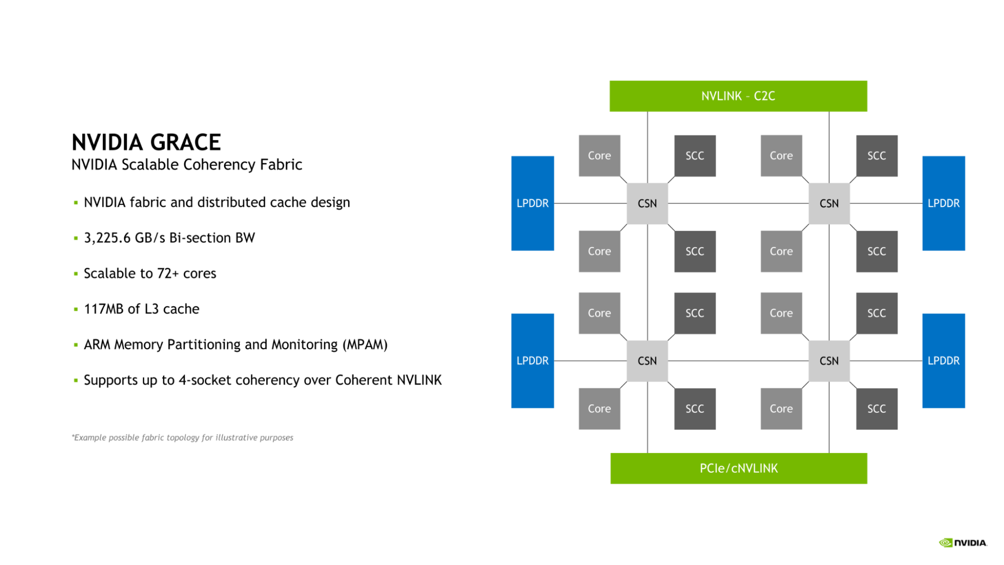
A single Grace CPU incorporates 72 CPU cores and 117 MB of cache, but SCF is designed for scalability beyond this configuration. When two Grace CPUs are combined to form a Grace Superchip, these figures double to 144 CPU cores and 234 MB of L3 cache, respectively.
The CPU cores and SCF Cache partitions (SCCs) are distributed throughout the mesh. Cache Switch Nodes (CSNs) route data through the fabric and serve as interfaces between the CPU cores, cache memory and the rest of the system, enabling high-bandwidth throughout.
Grace CPU incorporates support for Memory System Resource Partitioning and Monitoring (MPAM) capability, which is the Arm standard for partitioning both system cache and memory resources.
MPAM works by assigning partition IDs (PARTIDs) to requestors within the system. This design allows resources such as cache capacity and memory bandwidth to be partitioned or monitored based on their respective PARTIDs.
The SCF Cache in Grace CPU supports both the partitioning of cache capacity as well as memory bandwidth using MPAM. Additionally, Performance Monitor Groups (PMGs) can be used to monitor resource usage.
To deliver excellent bandwidth and energy efficiency, Grace CPU implements a 32-channel LPDDR5X memory interface. This provides memory capacity of up to 512 GB and memory bandwidth of up to 546 GB/s.
A key feature of the Grace Hopper Superchip is the introduction of Extended GPU Memory (EGM). By allowing any Hopper GPU connected from a larger NVLink network to access the LPDDR5X memory connected to the Grace CPU in the Grace Hopper Superchip, the memory pool available to the GPU is greatly expanded.
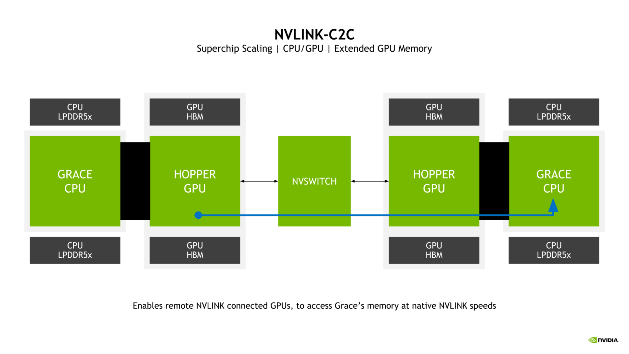
The GPU-to-GPU NVLink and NVLink-C2C bidirectional bandwidths are matched in a superchip, which enables the Hopper GPUs to access the Grace CPU memory at NVLink native speeds.
The selection of LPDDR5X for Grace CPU was driven by the need to strike the optimal balance of bandwidth, energy efficiency, capacity, and cost for large-scale AI and HPC workloads.
While a four-site HBM2e memory subsystem would have provided substantial memory bandwidth and good energy efficiency, it would do so at more than 3x the cost-per-gigabyte of either DDR5 or LPDDR5X.
Additionally, such a configuration would be limited to a capacity of only 64 GB, which is one-eighth the maximum capacity available to the Grace CPU with LPDDR5X.
Compared to a more traditional eight-channel DDR5 design, the Grace CPU LPDDR5X memory subsystem provides up to 53% more bandwidth and is substantially more power efficient, requiring just an eighth of the power per gigabyte.
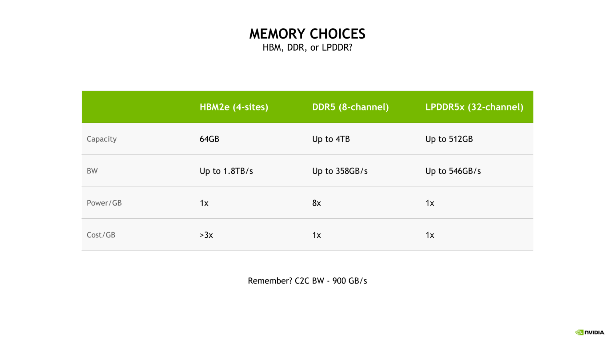
The excellent power efficiency of LPDDR5X enables allocating more of the total power budget to compute resources, such as the CPU cores or GPU streaming multiprocessors (SMs).
Grace CPU incorporates a complement of high-speed I/O to serve the needs of the modern data center. The Grace CPU SoC provides up to 68 lanes of PCIe connectivity and up to four PCIe Gen 5 x16 links. Each PCIe Gen 5 x16 link offers up to 128 GB/s of bidirectional bandwidth and can be further bifurcated into two PCIe Gen 5 x8 links for additional connectivity.
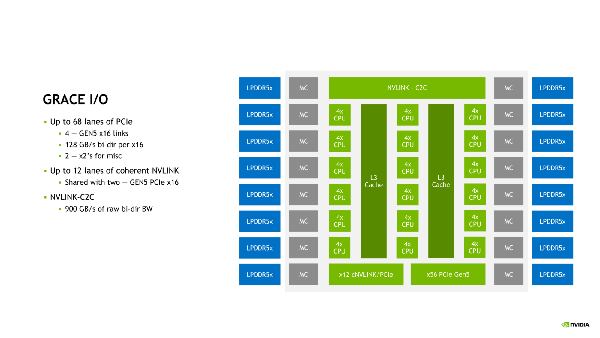
This connectivity is in addition to the on-die NVLink-C2C link that can be used to connect Grace CPU to either another Grace CPU or to an NVIDIA Hopper GPU.
The combination of NVLink, NVLink-C2C, and PCIe Gen 5 provides the Grace CPU with the rich suite of connectivity options and ample bandwidth needed to scale performance in the modern data center.
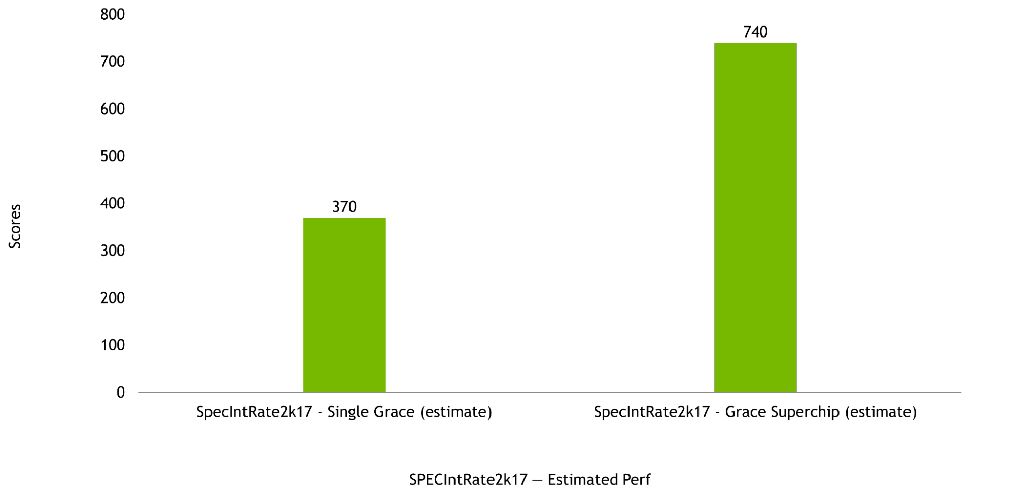
NVIDIA Grace CPU is designed to deliver excellent compute performance in both single-chip as well as Grace Superchip configurations, with estimated SPECrate2017_int_base scores of 370 and 740, respectively. These pre-silicon estimates are based on use of the GNU Compiler Collection (GCC).
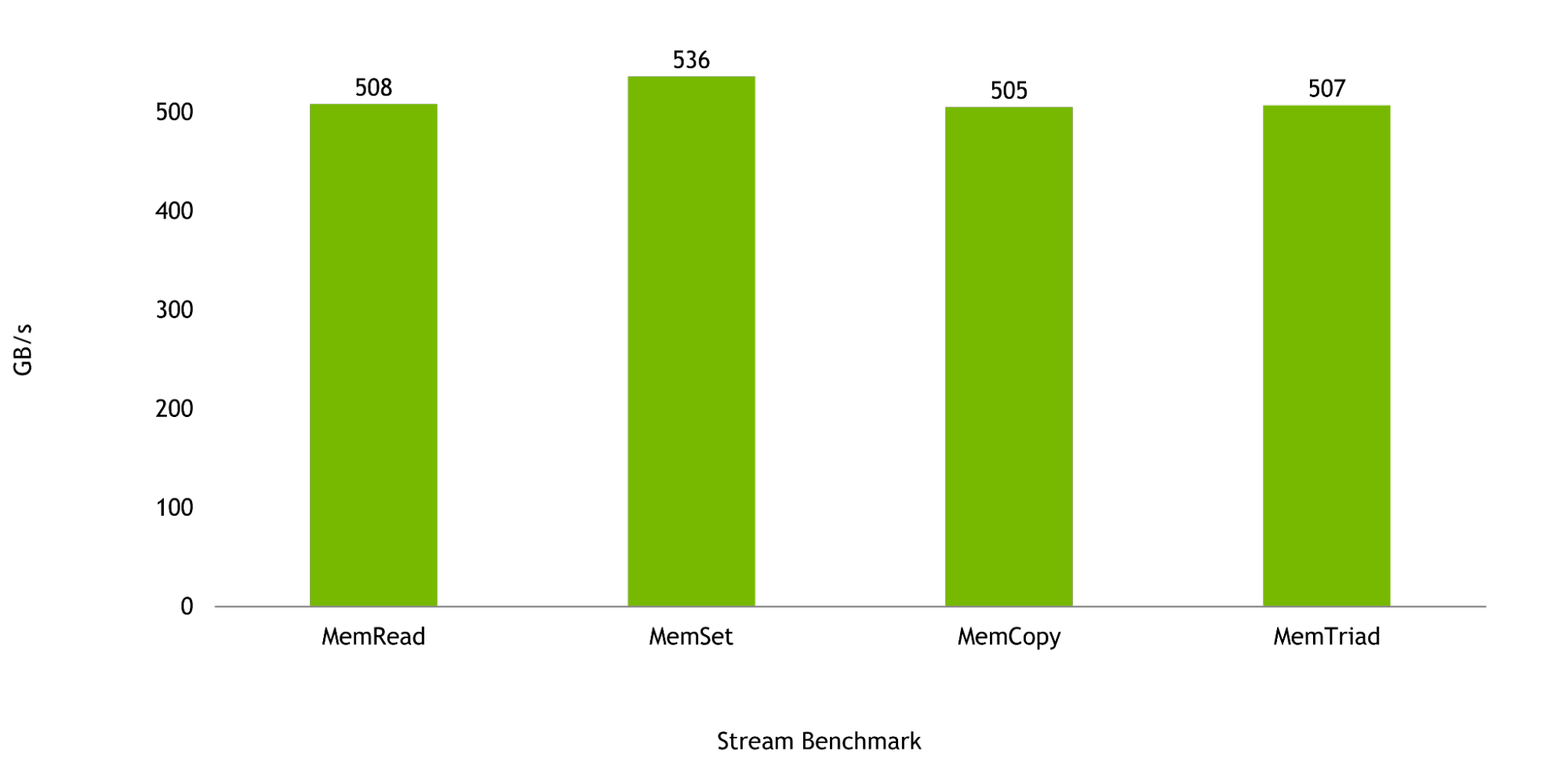
Memory bandwidth is critical to the workloads for which the Grace CPU was designed, and in the Stream Benchmark, a single Grace CPU is expected to deliver up to 536 GB/s of realized bandwidth, representing more than 98% of the chip’s peak theoretical bandwidth.
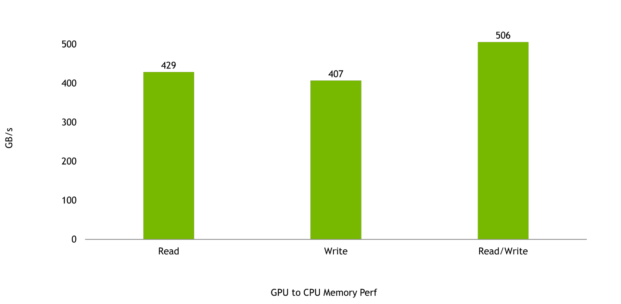
And, finally, the bandwidth between the Hopper GPU and the Grace CPU is critical to maximizing the performance of the Grace Hopper Superchip. GPU-to-CPU memory reads and writes are expected to be 429 GB/s and 407 GB/s, respectively, representing more than 95% and more than 90% of the peak theoretical unidirectional transfer rates of NVLink-C2C.
Combined read and write performance is expected to be 506 GB/s, representing over 92% of the peak theoretical memory bandwidth available to a single NVIDIA Grace CPU SoC.
With 144 cores and 1 TB/s of memory bandwidth, the NVIDIA Grace CPU Superchip will provide unprecedented performance for CPU-based high performance computing applications. HPC applications are compute-intensive, demanding the highest-performing cores, highest-memory bandwidth, and the right memory capacity per core to speed outcomes.
NVIDIA is working with leading HPC, supercomputing, hyperscale, and cloud customers for the Grace CPU Superchip. Grace CPU Superchip and Grace Hopper Superchip are expected to be available in the first half of 2023.
For more information about the NVIDIA Grace Hopper Superchip and NVIDIA Grace CPU Superchip, visit NVIDIA Grace CPU.
 Increasing demands in AI and high-performance computing (HPC) are driving a need for faster, more scalable interconnects with high-speed communication between…
Increasing demands in AI and high-performance computing (HPC) are driving a need for faster, more scalable interconnects with high-speed communication between every GPU.
The third-generation NVIDIA NVSwitch is designed to satisfy this communication need. This latest NVSwitch and the H100 Tensor Core GPU use the fourth-generation NVLink, the newest high-speed, point-to-point interconnect by NVIDIA.
The third-generation NVIDIA NVSwitch is designed to provide connectivity within a node or to GPUs external to the node for the NVLink Switch System. It also incorporates hardware acceleration for collective operations with multicast and NVIDIA Scalable Hierarchical Aggregation and Reduction Protocol (SHARP) in-network reductions.
NVIDIA NVSwitch is also a critical enabler of the NVLink Switch networking appliance, which enables the creation of clusters with up to 256 connected NVIDIA H100 Tensor Core GPUs and 57.6 TB/s of all-to-all bandwidth. The appliance delivers 9x more bisection bandwidth than was possible with HDR InfiniBand on NVIDIA Ampere Architecture GPUs.
The performance needs of AI and HPC workloads continue to grow rapidly and require scaling to multi-node, multi-GPU systems.
Delivering excellent performance at scale requires high-bandwidth communication between every GPU, and the NVIDIA NVLink specification is designed for synergistic operation with NVIDIA GPUs to enable the required performance and scalability.
For instance, the thread-block execution structure of NVIDIA GPUs efficiently feeds the parallelized NVLink architecture. NVLink-Port interfaces have also been designed to match the data exchange semantics of GPU L2 caches as closely as possible.
A key benefit of NVLink is that it offers substantially greater bandwidth than PCIe. Fourth-generation NVLink is capable of 100 Gbps per lane, more than tripling the 32 Gbps bandwidth of PCIe Gen5. Multiple NVLinks can be combined to provide even higher aggregate lane counts, yielding higher throughput.
NVLink has been designed specifically as a high-speed, point-to-point link to interconnect GPUs, yielding lower overhead than would be present in traditional networks.
This enables many of the complex networking features found in traditional networks—such as end-to-end retry, adaptive routing, and packet reordering—to be traded off for increased port counts.
The greater simplicity of the network interface allows for application–, presentation–, and session-layer functionality to be embedded directly into CUDA itself, further reducing communication overhead.
First introduced with the NVIDIA P100 GPU, NVLink has continued to advance in lockstep with NVIDIA GPU architectures, with each new architecture accompanied by a new generation of NVLink.
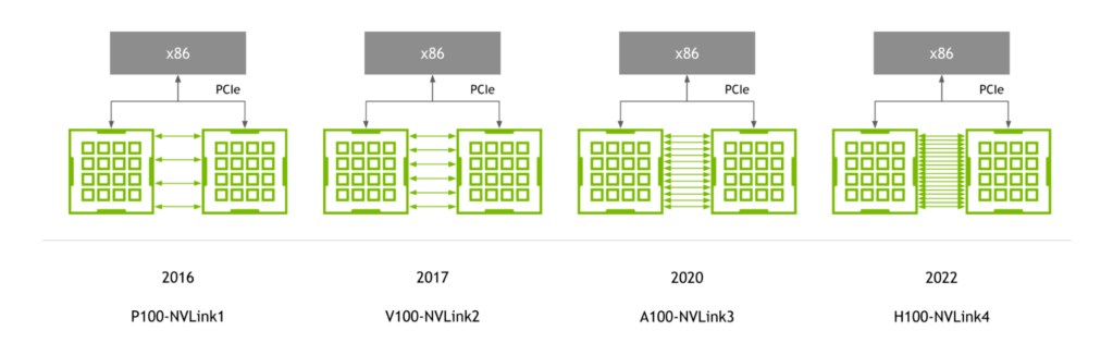
Fourth-generation NVLink provides 900 GB/s of bidirectional bandwidth per GPU—1.5x greater than the prior generation and more than 5.6x higher than first-generation NVLink.
NVIDIA NVSwitch was first introduced with the NVIDIA V100 Tensor Core GPU and second-generation NVLink, enabling high-bandwidth, any-to-any connectivity between all GPUs in a server.
The NVIDIA A100 Tensor Core GPU introduced third-generation NVLink and second-generation NVSwitch, doubling both per-GPU bandwidth as well as reduction bandwidth.
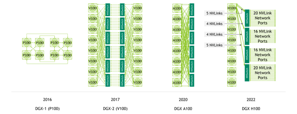
With fourth-generation NVLink and third-generation NVSwitch, a system with eight NVIDIA H100 Tensor Core GPUs features 3.6 TB/s of bisection bandwidth and 450 GB/s of bandwidth for reduction operations. These are1.5x and 3x increases compared to the prior generation.
In addition, with fourth-generation NVLink and third-generation NVSwitch as well as the external NVIDIA NVLink Switch, multi-GPU communication across multiple servers at NVLink speeds is now possible.
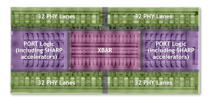
Third-generation NVSwitch is the largest NVSwitch to date. It is built using the TSMC 4N process customized for NVIDIA. The die incorporates 25.1 billion transistors—more transistors than the NVIDIA V100 Tensor Core GPU—in an area of 294 mm2. The package dimensions are 50 mm x 50 mm with a total of 2645 solder balls.
Third-generation NVSwitch is a key enabler of the NVLink Switch System, which enables connectivity between GPUs across nodes at NVLink speeds.
It incorporates physical (PHY) electrical interfaces that are compatible with 400 Gbps Ethernet and InfiniBand connectivity. The included management controller now provides support for attached Octal Small Formfactor Pluggable (OSFP) modules with four NVLinks per cage. With custom firmware, active cables can be supported.
Additional forward error correction (FEC) modes have also been added to enhance NVLink Network performance and reliability.
A security processor has also been added to protect data and chip configuration from attacks. The chip provides partitioning features that can isolate subsets of ports into separate NVLink Networks. Expanded telemetry features also enable InfiniBand-style monitoring.
Third-generation NVSwitch is our highest-bandwidth NVSwitch yet.
With 100 Gbps of bandwidth per differential pair using 50 Gbaud PAM4 signaling, third-generation NVSwitch provides 3.2 TB/s of full-duplex bandwidth across 64 NVLink ports (x2 per NVLink). It delivers more bandwidth in a system while also requiring fewer NVSwitch chips compared to the prior generation. All ports on third-generation NVSwitch are NVLink Network–capable.
Third-generation NVSwitch includes a host of new hardware blocks for SHARP acceleration:
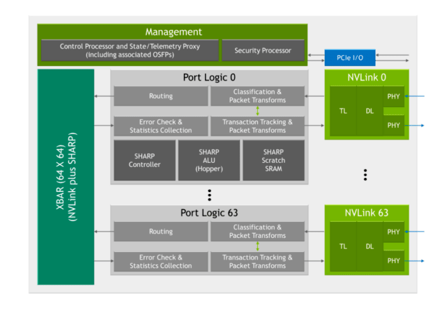
The embedded ALUs offer up to 400 FLOPS of FP32 throughput and have been added to perform reduction operations directly in NVSwitch, rather than by the GPUs in the system.
These ALUs support a wide variety of operators, such as logical, min/max, and add. They also support data formats such as signed/unsigned integers, FP16, FP32, FP64, and BF16.
Third-generation NVSwitch also includes a SHARP controller that can manage up to 128 SHARP groups in parallel. The crossbar bandwidth in the chip has been increased to carry additional SHARP-related exchanges.
A key use case for NVIDIA SHARP is for all-reduce operations that are common in AI training. When training networks using multiple GPUs, batches are split into smaller subbatches, which are then assigned to each individual GPU.
Each GPU processes their individual subbatches through the network parameters, yielding possible changes to the parameters, also known as local gradients. These local gradients are combined and reconciled to produce global gradients, which each GPU applies to their parameter tables. This averaging process is also known as an all-reduce operation.
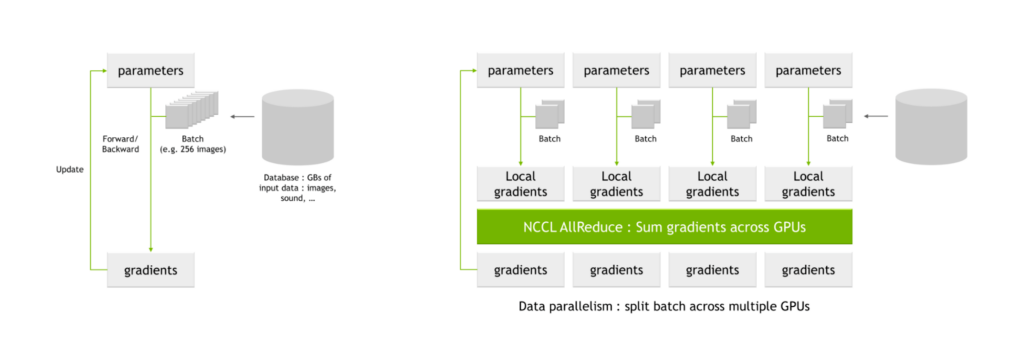
NVIDIA Magnum IO is the architecture for data center IO to accelerate multi-GPU and multi-node communications. It enables HPC, AI, and scientific applications to scale performance on new large GPU clusters scaled using NVLink and NVSwitch.
Magnum IO includes the NVIDIA Collective Communication Library (NCCL), which implements a wealth of multi-GPU and multi-node collective primitives, including all-reduce.
NCCL AllReduce takes as input the local gradients, partitions them into subsets, collects all subsets of a certain level and assigns it to a single GPU. The GPU then performs the reconciliation process for that subset, such as summing across local gradient values from all GPUs.
Following this process, a global set of gradients is produced and then distributed to all other GPUs.
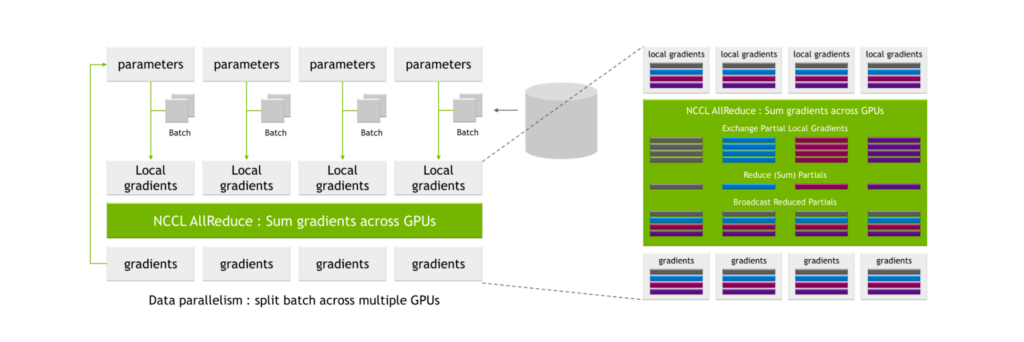
These processes are highly communication-intensive and the associated communication overhead can substantially lengthen the overall time to train.
With the NVIDIA A100 Tensor Core GPU, third-generation NVLink, and second-generation NVSwitch, the process of sending and receiving partials yields 2N reads (where N is the number of GPUs). The process of broadcasting results yields 2N writes for 2N reads and 2N writes at each GPU interface, or 4N total operations.
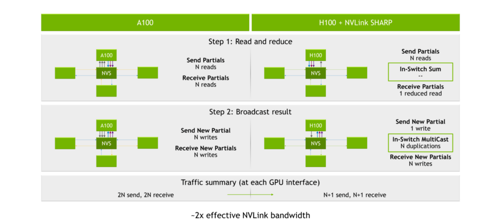
The SHARP engines are inside of third-generation NVSwitch. Instead of distributing the data to each GPU and having the GPUs perform the calculations, the GPUs send their data into third-generation NVSwitch chips. The chips then perform the calculations and then send the results back. This results in a total of 2N+2 operations, or approximately halving the number of read/write operations needed to perform the all-reduce calculation.
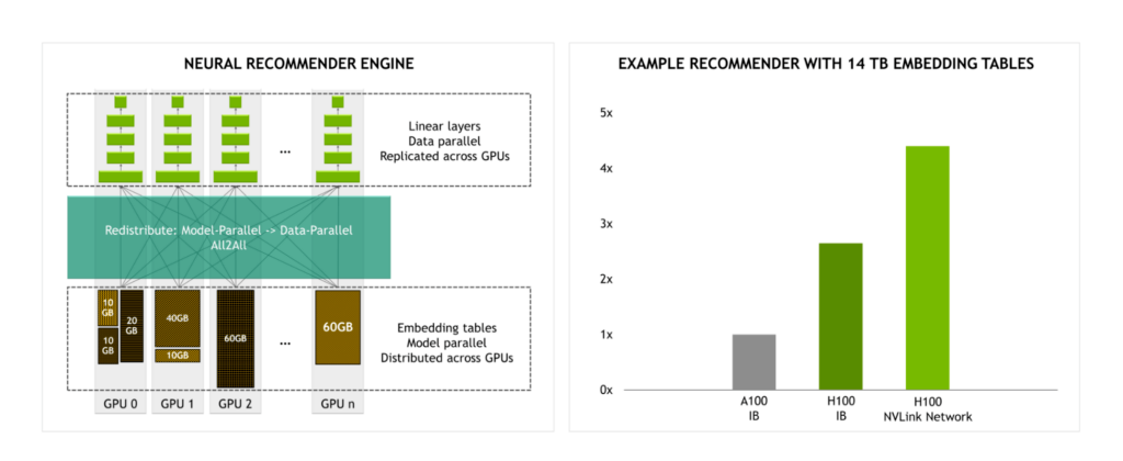
With the NVLink Switch System providing 4.5x more bandwidth than InfiniBand, large-scale model training becomes more practical.
For example, when training a recommendation engine with 14 TB embedding tables, we expect a significant performance uplift in performance for H100 using the NVLink Switch System compared to H100 using InfiniBand.
In prior generations of NVLink, each server had its own local address space used by GPUs within a server when communicating to each other over NVLink. With the NVLink Network, each server has its own address space, which is used when GPUs send data across the network, providing isolation and improved security when sharing data. This capability leverages functionality built into the latest NVIDIA Hopper GPU Architecture.
While NVLink performs connection setup during the system boot process, the NVLink Network connection setup is performed through a runtime API call by software. This enables the network to be reconfigured on the fly as different servers come online and as users enter and exit.
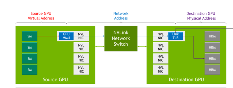
Table 1 shows how traditional networking concepts map to their counterparts in NVLink Network.
| Concept | Traditional Example | NVLink Network |
| Physical Layer | 400G electrical/optical media | Custom-FW OSFP |
| Data Link Layer | Ethernet | NVLink custom on-chip HW and FW |
| Network Layer | IP | New NVLink Network Addressing and Management Protocols |
| Transport Layer | TCP | NVLink custom on-chip HW and FW |
| Session Layer | Sockets | SHARP groupsCUDA export of Network addresses of data-structures |
| Presentation Layer | TSL/SSL | Library abstractions (e.g., NCCL, NVSHMEM) |
| Application Layer | HTTP/FTP | AI Frameworks or User Apps |
| NIC | PCIe NIC (card or chip) | Functions embedded in GPU and NVSwitch |
| RDMA Off-Load | NIC Off-Load Engine | GPU-internal Copy Engine |
| Collectives Off-Load | NIC/Switch Off-Load Engine | NVSwitch-internal SHARP Engines |
| Security Off-Load | NIC Security Features | GPU-internal Encryption and “TLB” Firewalls |
| Media Control | NIC Cable Adaptation | NVSwitch-internal OSFP-cable controllers |
NVIDIA DGX H100 is the latest iteration of the DGX family of systems based on the latest NVIDIA H100 Tensor Core GPU and incorporates:
Within a DGX H100, each of the eight H100 Tensor Core GPUs within the system is connected to all four third-generation NVSwitch chips. Traffic is sent across four different switch planes, enabling the aggregation of the links to achieve full all-to-all bandwidth between GPUs in the system.
With NVLink Network, all eight NVIDIA H100 Tensor Core GPUs within a server can half-subscribe 18 NVLinks to H100 Tensor Core GPUs in other servers.
Alternatively, four H100 Tensor Core GPUs in a server can fully subscribe 18 NVLinks to H100 Tensor Core GPUs in other servers. This 2:1 taper is a trade-off made to balance bandwidth with server complexity and cost for this instantiation of the technology.
With SHARP, the bandwidth delivered is equivalent to a full-bandwidth AllReduce.
Within a server, all eight GPUs independently support RDMA from their own dedicated 400 GB NICs. 800 GB/s of aggregate full-duplex bandwidth is possible to non-NVLink Network devices.
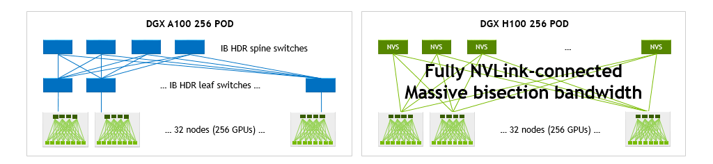
DGX H100 is the building block of the DGX H100 SuperPOD.
The NVLink Network provides 57.6 TB/s bisection bandwidth spanning the entire 256 GPUs. Additionally, the ConnectX-7s across all 32 DGXs and associated InfiniBand switches provide 25.6 TB/s of full duplex bandwidth for use within the pod or for scaling out the multiple SuperPODs.
A key enabler of DGX H100 SuperPOD is the new NVLink Switch based on the third-generation NVSwitch chips. DGX H100 SuperPOD includes 18 NVLink Switches.
The NVLink Switch fits in a standard 1U 19-inch form factor, significantly leveraging InfiniBand switch design, and includes 32 OSFP cages. Each switch incorporates two third-generation NVSwitch chips, providing 128 fourth-generation NVLink ports for an aggregate 6.4 TB/s full-duplex bandwidth.
NVLink Switch supports out-of-band management communication and a range of cabling options such as passive copper. With custom firmware, active copper and optical OSFP cables are also supported.
H100 SuperPOD with NVLink Network enables significant increases in bisection and reduce operation bandwidth compared to a DGX A100 SuperPOD with 256 DGX A100
GPUs.
A single DGX H100 delivers 1.5x the bisection and 3x the bandwidth for reduction operations of a single DGX A100. Those speedups grow to 9x and 4.5x in 32 DGX system configurations, each with a total of 256 GPUs.
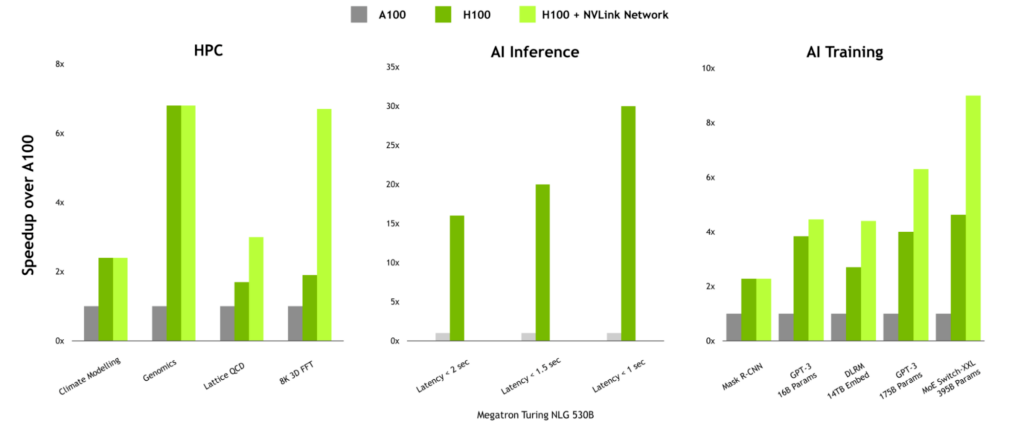
For workloads with high communication intensity, the performance benefits of NVLink Network can be significant. In HPC, workloads such as Lattice QCD and 8K 3D FFT see substantial benefits because multi-node scaling has been designed into the communication libraries within the HPC SDK and Magnum IO.
NVLink Network can also provide a significant boost when training large language models or recommenders with large embedding tables.
Delivering the highest performance for AI and HPC requires full-stack, data-center scale innovation. High-bandwidth, low-latency interconnect technologies are key enablers of performance at scale.
Third-generation NVSwitch delivers the next big leap for high-bandwidth, low-latency communication between GPUs both within a server, as well as bringing all-to-all GPU communication at full NVLink speed between server nodes.
Magnum IO works integrally with CUDA, HPC SDK, and nearly all deep learning frameworks. It enables AI software—such as large language models, recommender systems, and scientific applications like 3D FFT—to scale across multiple GPUs across multiple nodes using NVLink Switch System right out of the box.
For more information, see NVIDIA NVLink and NVSwitch.
 Ever since its introduction in CUDA 10, CUDA Graphs has been used in a variety of applications. A graph groups a set of CUDA kernels and other CUDA operations…
Ever since its introduction in CUDA 10, CUDA Graphs has been used in a variety of applications. A graph groups a set of CUDA kernels and other CUDA operations together and executes them with a specified dependency tree. It speeds up the workflow by combining the driver activities associated with CUDA kernel launches and CUDA API calls. It also enforces the dependencies with hardware accelerations, instead of relying solely on CUDA streams and events, when possible.
There are two main ways to construct a CUDA graph: explicit API calls and stream capture.
With this way of constructing a CUDA graph, nodes of the graph, formed by the CUDA kernel and CUDA memory operations, are added to the graph by calling the cudaGraphAdd*Node APIs, where * is replaced with the node type. Dependencies between the nodes are set explicitly with APIs.
The upside of constructing CUDA graphs with explicit APIs is that the cudaGraphAdd*Node APIs return node handles (cudaGraphNode_t) that can be used as references for future node updates. Kernel launch configurations and kernel function parameters of a kernel node in an instantiated graph, for example, can be updated with minimal cost with cudaGraphExecKernelNodeSetParams.
The downside is that in scenarios where CUDA graph is used to speed up existing code, constructing CUDA graphs with explicit API calls typically requires a significant number of code changes, especially changes regarding the control flow and function calling structure of the code.
With this way of constructing a CUDA graph, cudaStreamBeginCapture and cudaStreamEndCapture are placed before and after a code block. All device activities launched by the code block are recorded, captured, and grouped into a CUDA graph. The dependencies among the nodes are inferred from the CUDA stream or event API calls within the stream capture region.
The upside of constructing CUDA graphs with stream capture is that for existing code, fewer code changes are needed. The original code structure can be mostly untouched and graph construction is performed in an automatic way.
There are also downsides to this way of constructing CUDA graphs. Within the stream capture region, all kernel launch configurations and kernel function parameters, as well as the CUDA API call parameters are recorded by value. Whenever any of the configurations and parameters change, the captured and then instantiated graph becomes out-of-date.
Two solutions are provided in the Employing CUDA Graphs in a Dynamic Environment post:
There are, however, workflows where neither solution works well. The recapture-then-update approach works well on paper, but in some cases the recapture and update themselves are expensive. There are also cases where it is simply not possible to associate each set of parameters with a CUDA graph. For example, cases with floating-point number parameters are difficult to cache as there are huge numbers of possible floating-point numbers.
CUDA Graphs constructed with explicit APIs are easy to update but the approach can be too cumbersome and is less flexible. CUDA Graphs can be constructed flexibly with stream capture but the resulting graphs are difficult and expensive to update.
In this post, I provide an approach of constructing CUDA graphs with both the explicit API and stream capture methods, thus achieving the upsides of both and avoiding the downsides of either.
As an example, in a workflow where three kernels are launched sequentially, the first two kernels have static launch configurations and parameters, but the last kernel has a dynamic launch configuration and parameters.
Use stream capture to record the launches of the first two kernels and call explicit APIs to add the last kernel node to the capturing graph. The node handle returned by the explicit APIs is then used to update the instantiated graph with the dynamic configurations and parameters every time before the graph is launched.
The following code example shows the idea:
cudaStream_t stream;
std::vector _node_list;
cudaGraphExec_t _graph_exec;
if (not using_graph) {
  first_static_kernel>>(static_parameters);
  second_static_kernel>>(static_parameters);
  dynamic_kernel>>(dynamic_parameters);
} else {
  if (capturing_graph) {
    cudaStreamBeginCapture(stream, cudaStreamCaptureModeGlobal);
    first_static_kernel>>(static_parameters);
    second_static_kernel>>(static_parameters);

    // Get the current stream capturing graph

    cudaGraph_t _capturing_graph;
    cudaStreamCaptureStatus _capture_status;
    const cudaGraphNode_t *_deps;
    size_t _dep_count;
    cudaStreamGetCaptureInfo_v2(stream, &_capture_status, nullptr &_capturing_graph, &_deps, &_dep_count);

    // Manually add a new kernel node

    cudaGraphNode_t new_node;
    cudakernelNodeParams _dynamic_params_cuda;
    cudaGraphAddKernelNode(&new_node, _capturing_graph, _deps, _dep_count, &_dynamic_params_cuda);

    // ... and store the new node for future references

    _node_list.push_back(new_node);

    // Update the stream dependencies

    cudaStreamUpdateCaptureDependencies(stream, &new_node, 1, 1);

    // End the capture and instantiate the graph

    cudaGraph_t _captured_graph;
    cudaStreamEndCapture(stream, &_captured_graph);
    cudaGraphInstantiate(&_graph_exec, _captured_graph, nullptr, nullptr, 0);
  } else if (updating_graph) {
    cudakernelNodeParams _dynamic_params_updated_cuda;
    cudaGraphExecKernelNodeSetParams(_graph_exec, _node_list[0], &_dynamic_params_updated_cuda);
  }
} cudaStream_t stream;
std::vector _node_list;
cudaGraphExec_t _graph_exec;

if (not using_graph) {

  first_static_kernel>>(static_parameters);
  second_static_kernel>>(static_parameters);
  dynamic_kernel>>(dynamic_parameters);

} else {

  if (capturing_graph) {

    cudaStreamBeginCapture(stream, cudaStreamCaptureModeGlobal);

    first_static_kernel>>(static_parameters);
    second_static_kernel>>(static_parameters);

    // Get the current stream capturing graph
    cudaGraph_t _capturing_graph;
    cudaStreamCaptureStatus _capture_status;
    const cudaGraphNode_t *_deps;
    size_t _dep_count;
    cudaStreamGetCaptureInfo_v2(stream, &_capture_status, nullptr &_capturing_graph, &_deps, &_dep_count);

    // Manually add a new kernel node
    cudaGraphNode_t new_node;
    cudakernelNodeParams _dynamic_params_cuda;
    cudaGraphAddKernelNode(&new_node, _capturing_graph, _deps, _dep_count, &_dynamic_params_cuda);
    // ... and store the new node for future references
    _node_list.push_back(new_node);

    // Update the stream dependencies
    cudaStreamUpdateCaptureDependencies(stream, &new_node, 1, 1);

    // End the capture and instantiate the graph
    cudaGraph_t _captured_graph;
    cudaStreamEndCapture(stream, &_captured_graph);

    cudaGraphInstantiate(&_graph_exec, _captured_graph, nullptr, nullptr, 0);

  } else if (updating_graph) {
    cudakernelNodeParams _dynamic_params_updated_cuda;

    cudaGraphExecKernelNodeSetParams(_graph_exec, _node_list[0], &_dynamic_params_updated_cuda);

  }
}
cudaStream_t stream;
std::vector _node_list;
cudaGraphExec_t _graph_exec;
if (not using_graph) {
  first_static_kernel>>(static_parameters);
  second_static_kernel>>(static_parameters);
  dynamic_kernel>>(dynamic_parameters);
} else {
  if (capturing_graph) {
    cudaStreamBeginCapture(stream, cudaStreamCaptureModeGlobal);
    first_static_kernel>>(static_parameters);
    second_static_kernel>>(static_parameters);

    // Get the current stream capturing graph

    cudaGraph_t _capturing_graph;
    cudaStreamCaptureStatus _capture_status;
    const cudaGraphNode_t *_deps;
    size_t _dep_count;
    cudaStreamGetCaptureInfo_v2(stream, &_capture_status, nullptr &_capturing_graph, &_deps, &_dep_count);

    // Manually add a new kernel node

    cudaGraphNode_t new_node;
    cudakernelNodeParams _dynamic_params_cuda;
    cudaGraphAddKernelNode(&new_node, _capturing_graph, _deps, _dep_count, &_dynamic_params_cuda);

    // ... and store the new node for future references

    _node_list.push_back(new_node);

    // Update the stream dependencies

    cudaStreamUpdateCaptureDependencies(stream, &new_node, 1, 1);

    // End the capture and instantiate the graph

    cudaGraph_t _captured_graph;
    cudaStreamEndCapture(stream, &_captured_graph);
    cudaGraphInstantiate(&_graph_exec, _captured_graph, nullptr, nullptr, 0);
  } else if (updating_graph) {
    cudakernelNodeParams _dynamic_params_updated_cuda;
    cudaGraphExecKernelNodeSetParams(_graph_exec, _node_list[0], &_dynamic_params_updated_cuda);
  }
}
In this example, cudaStreamGetCaptureInfo_v2 extracts the CUDA graph that is currently being recorded and captured into. A kernel node is added to this graph with the node handle (new_node) returned and stored, before cudaStreamUpdateCaptureDependencies is called to update the dependency tree of the current capturing stream. The last step is necessary to ensure that any other activities captured afterward have their dependencies set on these manually added nodes correctly.
With this approach, the same instantiated graph (cudaGraphExec_t object) can be reused directly with a lightweight cudaGraphExecKernelNodeSetParams call, even though the parameters are dynamic. The first image in this post shows this usage.
Furthermore, the capture and update code paths can be combined into one piece of code that lives next to the original code that launches the last two kernels. This inflicts a minimal number of code changes and does not break the original control flow and function call structure.
The new approach is shown in detail in the hummingtree/cuda-graph-with-dynamic-parameters standalone code example. cudaStreamGetCaptureInfo_v2 and cudaStreamUpdateCaptureDependencies are new CUDA runtime APIs introduced in CUDA 11.3.
Using the hummingtree/cuda-graph-with-dynamic-parameters standalone code example, I measured the performance of running the same dynamic workflow that is bound by kernel launch overhead with three different approaches:
Table 1 shows the results. The speedup from the approaches mentioned in this post strongly depends on the underlying workflow.
| Approach | Time | Speedup over no graph |
| Combined | 433 ms | 1.63 |
| Recapture-then-update | 580 ms | 1.22 |
| No CUDA Graph | 706 ms | 1.00 |
In this post, I introduced an approach to constructing CUDA graphs that combines both the explicit API and stream capture methods. It provides a way to reuse instantiated graphs for workflows with dynamic parameters at minimal cost.
In addition to the CUDA technical posts mentioned earlier, the CUDA Graph section of the CUDA Programming Guide provides a comprehensive introduction to CUDA Graphs and its usages. For useful tips on employing CUDA Graphs in various applications, see the Nearly Effortless CUDA Graphs GTC session.
Online video sharing platforms, like YouTube, need to understand perceptual video quality (i.e., a user’s subjective perception of video quality) in order to better optimize and improve user experience. Video quality assessment (VQA) attempts to build a bridge between video signals and perceptual quality by using objective mathematical models to approximate the subjective opinions of users. Traditional video quality metrics, like peak signal-to-noise ratio (PSNR) and Video Multi-Method Assessment Fusion (VMAF), are reference-based and focus on the relative difference between the target and reference videos. Such metrics, which work best on professionally generated content (e.g., movies), assume the reference video is of pristine quality and that one can induce the target video’s absolute quality from the relative difference.
However, the majority of the videos that are uploaded on YouTube are user-generated content (UGC), which bring new challenges due to their remarkably high variability in video content and original quality. Most UGC uploads are non-pristine and the same amount of relative difference could imply very different perceptual quality impacts. For example, people tend to be less sensitive to the distortions of poor quality uploads than of high quality uploads. Thus, reference-based quality scores become inaccurate and inconsistent when used for UGC cases. Additionally, despite the high volume of UGC, there are currently limited UGC video quality assessment (UGC-VQA) datasets with quality labels. Existing UGC-VQA datasets are either small in size (e.g., LIVE-Qualcomm has 208 samples captured from 54 unique scenes), compared with datasets with millions of samples for classification and recognition (e.g., ImageNet and YouTube-8M), or don’t have enough content variability (sampling without considering content information, like LIVE-VQC and KoNViD-1k).
In “Rich Features for Perceptual Quality Assessment of UGC Videos“, published at CVPR 2021, we describe how we attempt to solve the UGC quality assessment problem by building a Universal Video Quality (UVQ) model that resembles a subjective quality assessment. The UVQ model uses subnetworks to analyze UGC quality from high-level semantic information to low-level pixel distortions, and provides a reliable quality score with rationale (leveraging comprehensive and interpretable quality labels). Moreover, to advance UGC-VQA and compression research, we enhance the open-sourced YouTube-UGC dataset, which contains 1.5K representative UGC samples from millions of UGC videos (distributed under the Creative Commons license) on YouTube. The updated dataset contains ground-truth labels for both original videos and corresponding transcoded versions, enabling us to better understand the relationship between video content and its perceptual quality.
Subjective Video Quality Assessment
To understand perceptual video quality, we leverage an internal crowd-sourcing platform to collect mean opinion scores (MOS) with a scale of 1–5, where 1 is the lowest quality and 5 is the highest quality, for no-reference use cases. We collect ground-truth labels from the YouTube-UGC dataset and categorize UGC factors that affect quality perception into three high-level categories: (1) content, (2) distortions, and (3) compression. For example, a video with no meaningful content won’t receive a high quality MOS. Also, distortions introduced during the video production phase and video compression artifacts introduced by third-party platforms, e.g., transcoding or transmission, will degrade the overall quality.
 |
 |
| MOS= 2.052 | MOS= 4.457 |
| Left: A video with no meaningful content won’t receive a high quality MOS. Right: A video displaying intense sports shows a higher MOS. |
 |
 |
| MOS= 1.242 | MOS= 4.522 |
| Left: A blurry gaming video gets a very low quality MOS. Right: A video with professional rendering (high contrast and sharp edges, usually introduced in the video production phase) shows a high quality MOS. |
 |
 |
| MOS= 2.372 | MOS= 4.646 |
| Left: A heavily compressed video receives a low quality MOS. Right: a video without compression artifacts shows a high quality MOS. |
We demonstrate that the left gaming video in the second row of the figure above has the lowest MOS (1.2), even lower than the video with no meaningful content. A possible explanation is that viewers may have higher video quality expectations for videos that have a clear narrative structure, like gaming videos, and the blur artifacts significantly reduce the perceptual quality of the video.
UVQ Model Framework
A common method for evaluating video quality is to design sophisticated features, and then map these features to a MOS. However, designing useful handcrafted features is difficult and time-consuming, even for domain experts. Also, the most useful existing handcrafted features were summarized from limited samples, which may not perform well on broader UGC cases. In contrast, machine learning is becoming more prominent in UGC-VQA because it can automatically learn features from large-scale samples.
A straightforward approach is to train a model from scratch on existing UGC quality datasets. However, this may not be feasible as there are limited quality UGC datasets. To overcome this limitation, we apply a self-supervised learning step to the UVQ model during training. This self-supervised step enables us to learn comprehensive quality-related features, without ground-truth MOS, from millions of raw videos.
Following the quality-related categories summarized from the subjective VQA, we develop the UVQ model with four novel subnetworks. The first three subnetworks, which we call ContentNet, DistortionNet and CompressionNet, are used to extract quality features (i.e., content, distortion and compression), and the fourth subnetwork, called AggregationNet, maps the extracted features to generate a single quality score. ContentNet is trained in a supervised learning fashion with UGC-specific content labels that are generated by the YouTube-8M model. DistortionNet is trained to detect common distortions, e.g., Gaussian blur and white noise of the original frame. CompressionNet focuses on video compression artifacts, whose training data are videos compressed with different bitrates. CompressionNet is trained using two compressed variants of the same content that are fed into the model to predict corresponding compression levels (with a higher score for more noticeable compression artifacts), with the implicit assumption that the higher bitrate version has a lower compression level.
The ContentNet, DistortionNet and CompressionNet subnetworks are trained on large-scale samples without ground-truth quality scores. Since video resolution is also an important quality factor, the resolution-sensitive subnetworks (CompressionNet and DistortionNet) are patch-based (i.e., each input frame is divided into multiple disjointed patches that are processed separately), which makes it possible to capture all detail on native resolution without downscaling. The three subnetworks extract quality features that are then concatenated by the fourth subnetwork, AggregationNet, to predict quality scores with domain ground-truth MOS from YouTube-UGC.
 |
| The UVQ training framework. |
Analyzing Video Quality with UVQ
After building the UVQ model, we use it to analyze the video quality of samples pulled from YouTube-UGC and demonstrate that its subnetworks can provide a single quality score along with high-level quality indicators that can help us understand quality issues. For example, DistortionNet detects multiple visual artifacts, e.g., jitter and lens blur, for the middle video below, and CompressionNet detects that the bottom video has been heavily compressed.
 |
| ContentNet assigns content labels with corresponding probabilities in parentheses, i.e., car (0.58), vehicle (0.42), sports car (0.32), motorsports (0.18), racing (0.11). |
 |
| DistortionNet detects and categorizes multiple visual distortions with corresponding probabilities in parentheses, i.e., jitter (0.112), color quantization (0.111), lens blur (0.108), denoise (0.107). |
 |
| CompressionNet detects a high compression level of 0.892 for the video above. |
Additionally, UVQ can provide patch-based feedback to locate quality issues. Below, UVQ reports that the quality of the first patch (patch at time t = 1) is good with a low compression level. However, the model identifies heavy compression artifacts in the next patch (patch at time t = 2).
 |
 |
 |
| Patch at time t = 1 | Patch at time t = 2 |
| Compression level = 0.000 | Compression level = 0.904 |
| UVQ detects a sudden quality degradation (high compression level) for a local patch. |
In practice, UVQ can generate a video diagnostic report that includes a content description (e.g., strategy video game), distortion analysis (e.g., the video is blurry or pixelated) and compression level (e.g., low or high compression). Below, UVQ reports that the content quality, looking at individual features, is good, but the compression and distortion quality is low. When combining all three features, the overall quality is medium-low. We see that these findings are close to the rationale summarized by internal user experts, demonstrating that UVQ can reason through quality assessments, while providing a single quality score.
 |
| UVQ diagnostic report. ContentNet (CT): Video game, strategy video game, World of Warcraft, etc. DistortionNet (DT): multiplicative noise, Gaussian blur, color saturation, pixelate, etc. CompressionNet (CP): 0.559 (medium-high compression). Predicted quality score in [1, 5]: (CT, DT, CP) = (3.901, 3.216, 3.151), (CT+DT+CP) = 3.149 (medium-low quality). |
Conclusion
We present the UVQ model, which generates a report with quality scores and insights that can be used to interpret UGC video perceptual quality. UVQ learns comprehensive quality related features from millions of UGC videos and provides a consistent view of quality interpretation for both no-reference and reference cases. To learn more, read our paper or visit our website to see YT-UGC videos and their subjective quality data. We also hope that the enhanced YouTube-UGC dataset enables more research in this space.
Acknowledgements
This work was possible through a collaboration spanning several Google teams. Key contributors include: Balu Adsumilli, Neil Birkbeck, Joong Gon Yim from YouTube and Junjie Ke, Hossein Talebi, Peyman Milanfar from Google Research. Thanks to Ross Wolf, Jayaprasanna Jayaraman, Carena Church, and Jessie Lin for their contributions.
AI Centers of Excellence are organizational units dedicated to implementing a company-wide AI vision. They help identify business use cases, create an implementation roadmap, accelerate adoption, assess impact and more. NVIDIA GTC, a global conference on AI and the metaverse, brings together the world’s top business and technology leaders who’ve embraced artificial intelligence to transform Read article >
The post Learn How Leading Companies Are Building AI Centers of Excellence, at NVIDIA GTC appeared first on NVIDIA Blog.
") Discover the latest innovations in AI and robotics, and hear world-renowned roboticist Dr. Henrik Christensen talk about the future of robotics.
Discover the latest innovations in AI and robotics, and hear world-renowned roboticist Dr. Henrik Christensen talk about the future of robotics.
Discover the latest innovations in AI and robotics, and hear world-renowned roboticist Dr. Henrik Christensen talk about the future of robotics.
Recent AI advances enable modeling of weather forecasting 4-5 magnitudes faster than traditional computing methods. The brightest leaders, researchers and developers in climate science, high performance computing and AI will discuss such technology breakthroughs — and how they can help foster a greener Earth — at NVIDIA GTC. The virtual conference, running Sept. 19-22, also Read article >
The post Predict, Detect, Mitigate: AI for Climate Science Takes the Stage at NVIDIA GTC appeared first on NVIDIA Blog.
Floods in Kentucky and wildfires in California are the kinds of disasters companies of all sorts are trying to address with AI. Tom Rikert, co-founder and CEO of San Francisco-based startup Masterful AI, is one of many experts helping them manage catastrophe risk. In the U.S. alone, the National Association of Insurance Commissioners estimates that Read article >
The post Shelter From the Storm: AI Helps Gauge Catastrophe Risks appeared first on NVIDIA Blog.
A triple threat steps In the NVIDIA Studio this week: a tantalizing trio of talented 3D artists who each reimagined and remastered classic European buildings with individualistic flair.
The post 3D Artists Reimagine, Remaster Iconic European Architecture This Week ‘In the NVIDIA Studio’ appeared first on NVIDIA Blog.